
TL;DR — What You Need to Know in 30 Seconds
Wearable device development demands a unique blend of miniaturized hardware, biocompatible materials, and ultra-low-power design. This guide covers market trends, core design challenges, manufacturing considerations, and certification requirements. Whether you are building a fitness tracker, a medical-grade monitor, or a smart ring, these insights will help you navigate the path from concept to certified mass production.
Why Wearable Device Development Is Different
Notably, wearable devices occupy a distinct category in hardware product development. Unlike conventional consumer electronics, wearables must conform to the human body. Therefore, every design decision works within extreme size and weight constraints.
Additionally, wearables operate in direct contact with skin for extended periods. This introduces biocompatibility requirements that standard electronics never face. A product strategy session for a wearable project must address these constraints from day one.
The convergence of health monitoring, AI processing, and connectivity further compounds the challenge. Founders must balance sensor accuracy, battery life, and form factor simultaneously. Consequently, these trade-offs often determine market success or failure before manufacturing even begins.
Wearable development also spans more disciplines than typical hardware projects. Teams need expertise in industrial design, mechanical engineering, embedded firmware, RF engineering, and regulatory compliance. Moreover, the compact form factor means these disciplines must collaborate more tightly than in larger products.
The Wearable Market in 2026: Key Trends
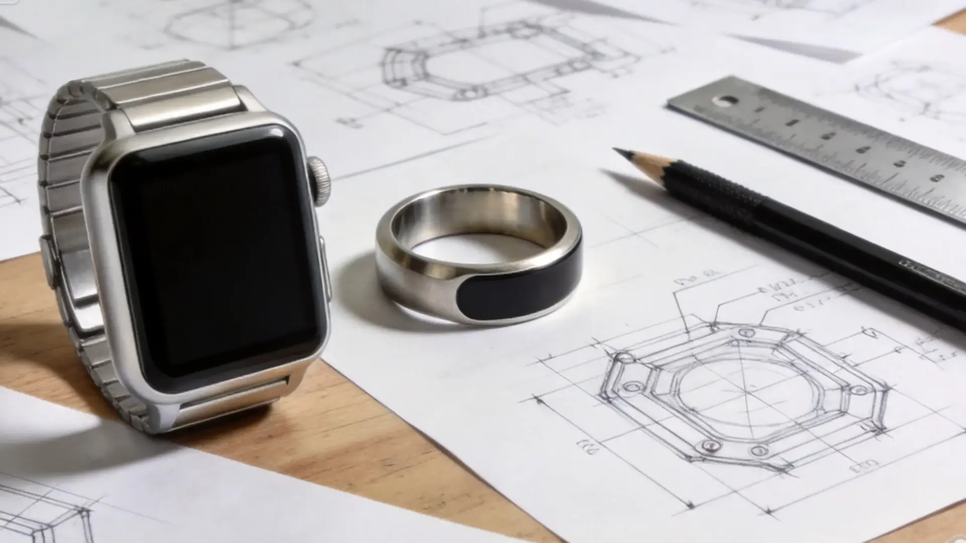
The global wearable technology market is projected to reach $91.1 billion in 2026, according to GM Insights. Meanwhile, total shipments are forecast to grow at a 2.6% CAGR through 2030, reaching approximately 693 million units, as reported by IDC.
Several trends are reshaping the competitive landscape. First, smart glasses are the fastest-growing form factor, with shipments up 41.4% year over year to 13.6 million units. This growth is driven by display-less AI glasses from both established players and new entrants. Second, smart rings continue gaining ground at 4.9 million units, as Oura faces increasing competition. Third, medical-grade wearables are growing at a 34% CAGR, driven by demand for continuous health monitoring.
Moreover, AI at the edge is moving from trials to operational reality. Qualcomm’s Snapdragon Wear Elite platform, launched in 2026, enables on-device inference for wearables. This shift reduces cloud dependency and lowers latency for critical health alerts. Meanwhile, Bluetooth 6.0 is entering commercial deployment, extending range to 400 meters and improving multi-device synchronization by 50%.
For hardware founders, these trends signal a clear direction. The market rewards specialized, purpose-built devices over generic feature-stuffed wearables. Therefore, industrial design choices must align with a sharply defined use case from the start.
Core Design Challenges in Wearable Device Development
Form Factor and Ergonomics
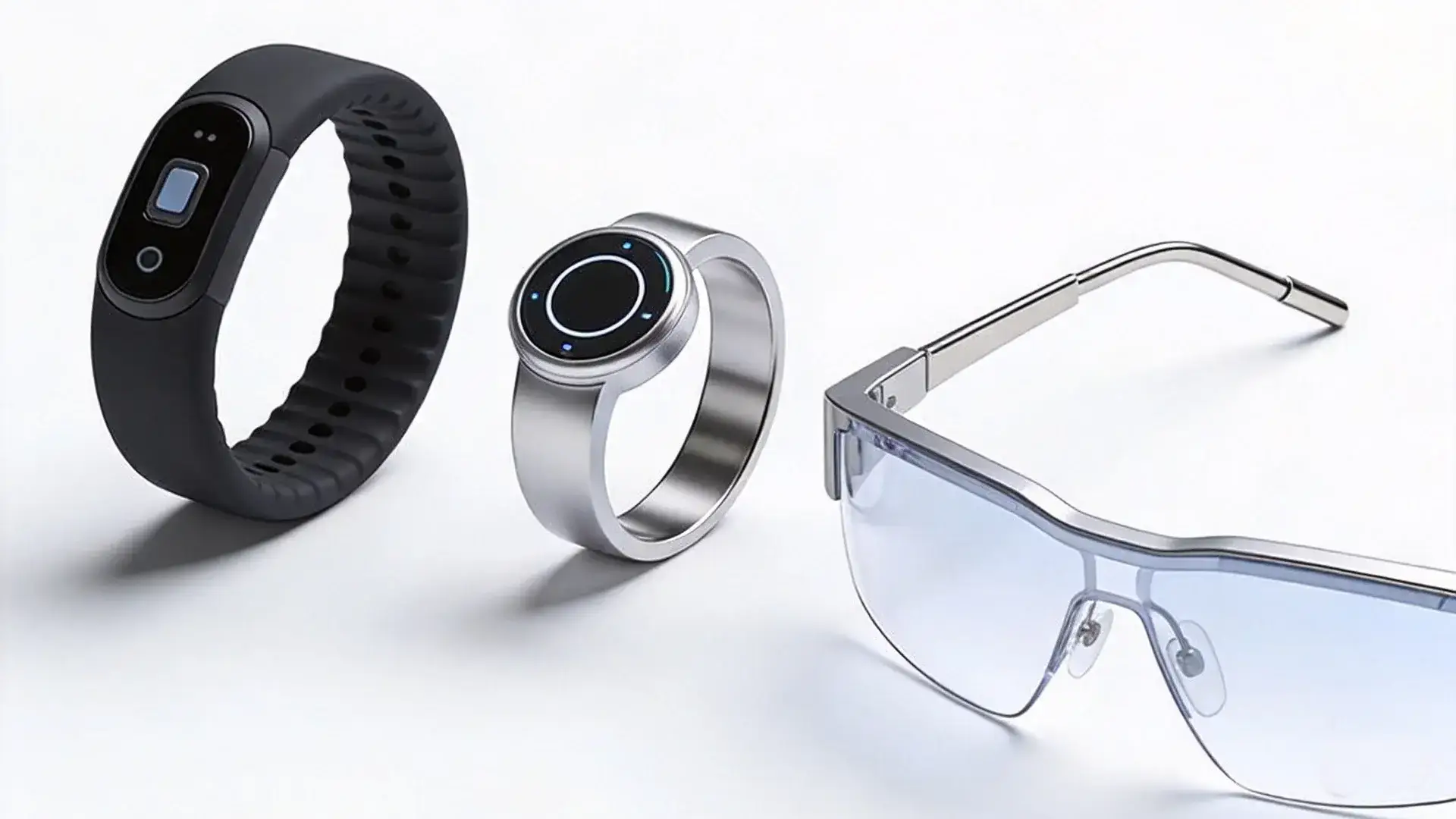
Specifically, the physical form of a wearable device dictates user acceptance. A device that feels bulky or uncomfortable will be abandoned, regardless of its technical capabilities. Therefore, ergonomics must drive the mechanical design process from the earliest concept sketches.
Key considerations include weight distribution, skin contact pressure, and thermal dissipation. Devices worn on the wrist, finger, or face each present unique ergonomic constraints. For example, a smart ring must accommodate finger swelling throughout the day while maintaining consistent sensor contact.
Importantly, material selection plays a critical role in wearable comfort. Biocompatible materials like medical-grade silicone, titanium, and hypoallergenic polymers are essential for skin-contact surfaces. Furthermore, adhesive patches for continuous monitoring devices require careful selection between acrylate, silicone, and polyurethane options. Each material presents different trade-offs in adhesion strength, skin safety, and durability under humid conditions.
Thermal management is equally important in wearable device development. Components generate heat that transfers directly to the user’s skin. Therefore, thermal simulations must verify that surface temperatures stay within safe limits during sustained operation. This is particularly critical for devices with high-power sensors or wireless charging.
Power Management: The Persistent Bottleneck
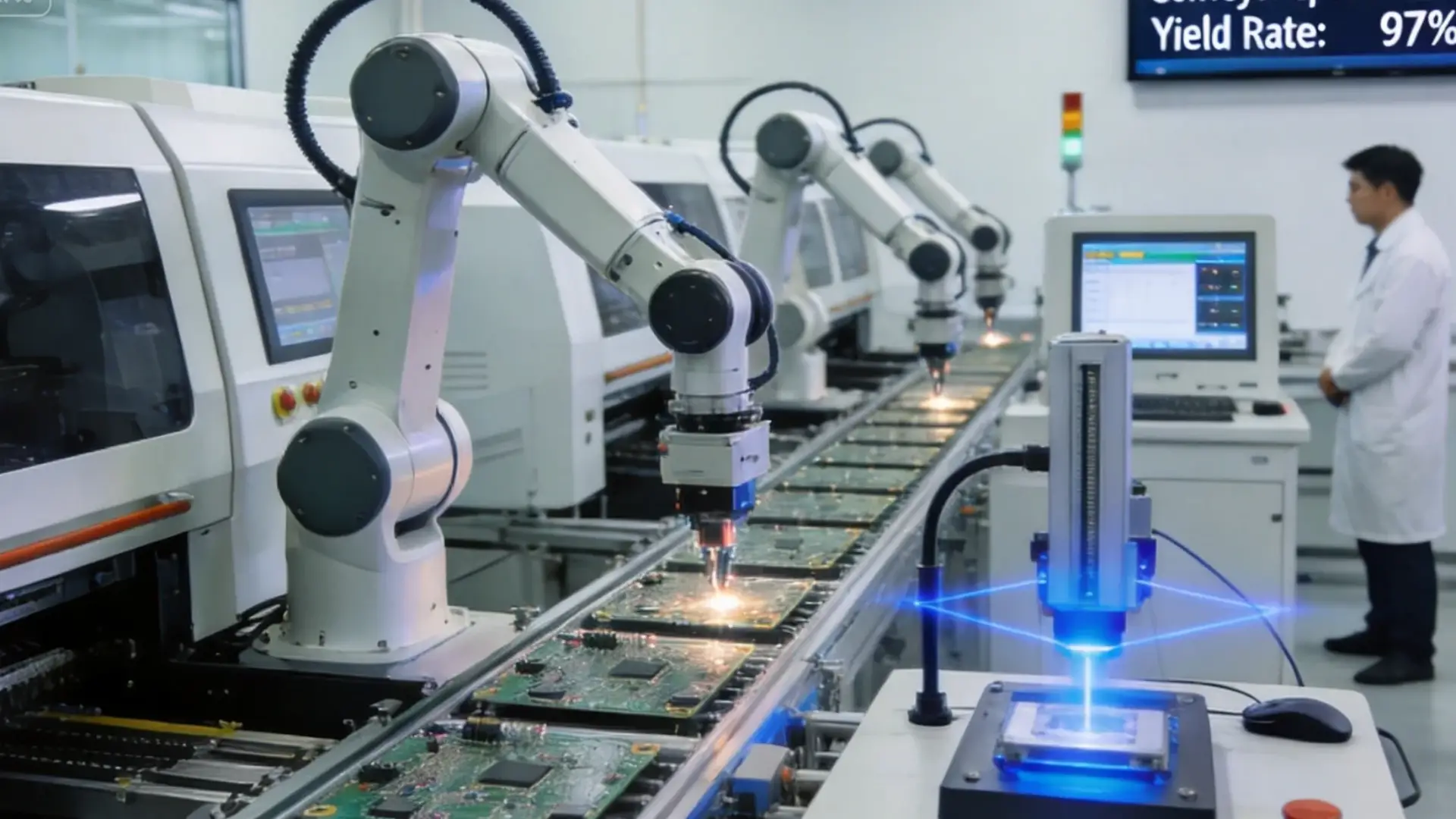
Importantly, power remains the most stubborn bottleneck in wearable device development. The continuous operation of multiple sensors, wireless communication, and data processing places enormous strain on limited battery capacity. According to research published in Advanced Energy and Sustainability Research, most healthcare wearables still rely on batteries fundamentally misaligned with their operational demands.
Several strategies help address this challenge. Duty cycling allows sensors to wake only when needed, sleeping between measurements. Edge processing enables local inference, reducing cloud round-trips and saving power. Multi-protocol connectivity uses BLE for pairing, Thread for low-power mesh, and Wi-Fi only for high-bandwidth transfers.
Additionally, power management integrated circuits play a crucial role in modern wearable designs. These chips orchestrate voltage regulation, battery charging, and power sequencing across multiple subsystems. Target Wake Time in Wi-Fi 6 further reduces consumption by scheduling data exchanges and letting radios sleep between intervals.
Hardware design teams must model power budgets early in development. A realistic power analysis during the prototyping phase prevents costly late-stage redesigns. Moreover, emerging energy harvesting technologies offer promising pathways to reduce battery dependence entirely.
Sensor Integration and Data Quality
Notably, multi-sensor fusion is the backbone of modern wearable functionality. Combining data from accelerometers, gyroscopes, PPG sensors, and temperature probes enables richer insights. However, integration introduces significant technical challenges.
Signal dropout, sensor drift, and motion artifacts all degrade data quality. Furthermore, placing multiple sensors in a compact enclosure creates electromagnetic interference. A peer-reviewed study in the journal Electronics highlights how poor skin contact and environmental interference compromise data integrity in wearable systems.
To mitigate these issues, founders should implement several safeguards. First, select sensors with built-in calibration capabilities. Second, develop software-based drift compensation algorithms. Third, design mechanical structures that maintain consistent skin pressure across different body types. Finally, conduct extensive real-world testing across diverse user demographics and activity levels.
Sensor calibration also extends into manufacturing. Each unit requires individual calibration under standardized lighting conditions to ensure consistent performance. This step adds time and cost to production but is essential for devices making health-related measurements.
Hardware Architecture for Wearable Devices
Connectivity Protocol Selection
Consequently, modern wearables must support multiple wireless protocols simultaneously. Bluetooth Low Energy handles initial pairing and low-bandwidth communication. Wi-Fi enables firmware updates and data synchronization. Thread provides low-power mesh connectivity for smart home integration.
However, running multiple radios on the 2.4 GHz spectrum creates interference. Without advanced filtering, signals collide and packets drop. The solution is consolidating radios onto a single system-on-chip. On a single die, arbitration happens in nanoseconds rather than milliseconds, preventing collisions.
This is where software design expertise becomes critical. Firmware must manage radio coexistence, power state transitions, and sensor polling schedules. All of these tasks must execute within tight latency budgets. Furthermore, the firmware must handle OTA updates securely, ensuring device integrity throughout the product lifecycle.
Miniaturization and PCB Design
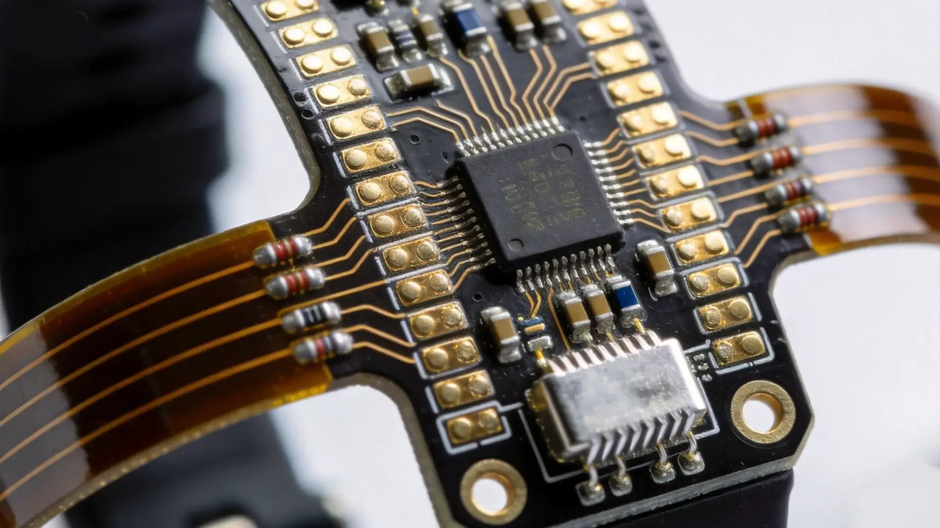
Specifically, wearable PCBs demand exceptional component density. Parts must fit within tiny enclosures while maintaining signal integrity and thermal performance. Rigid-flex PCB technology is often necessary to conform to curved device geometries.
Key PCB design considerations include component placement to minimize trace length. Shielding strategies protect RF-sensitive analog circuits from digital noise. Thermal vias dissipate heat from power-dense components. Additionally, antenna clearance and ground plane optimization require careful electromagnetic simulation.
The design for assembly principles become especially important in wearable manufacturing. Fewer assembly steps and simpler fastening methods reduce both cost and failure points in miniature devices.
Manufacturing Considerations for Wearables
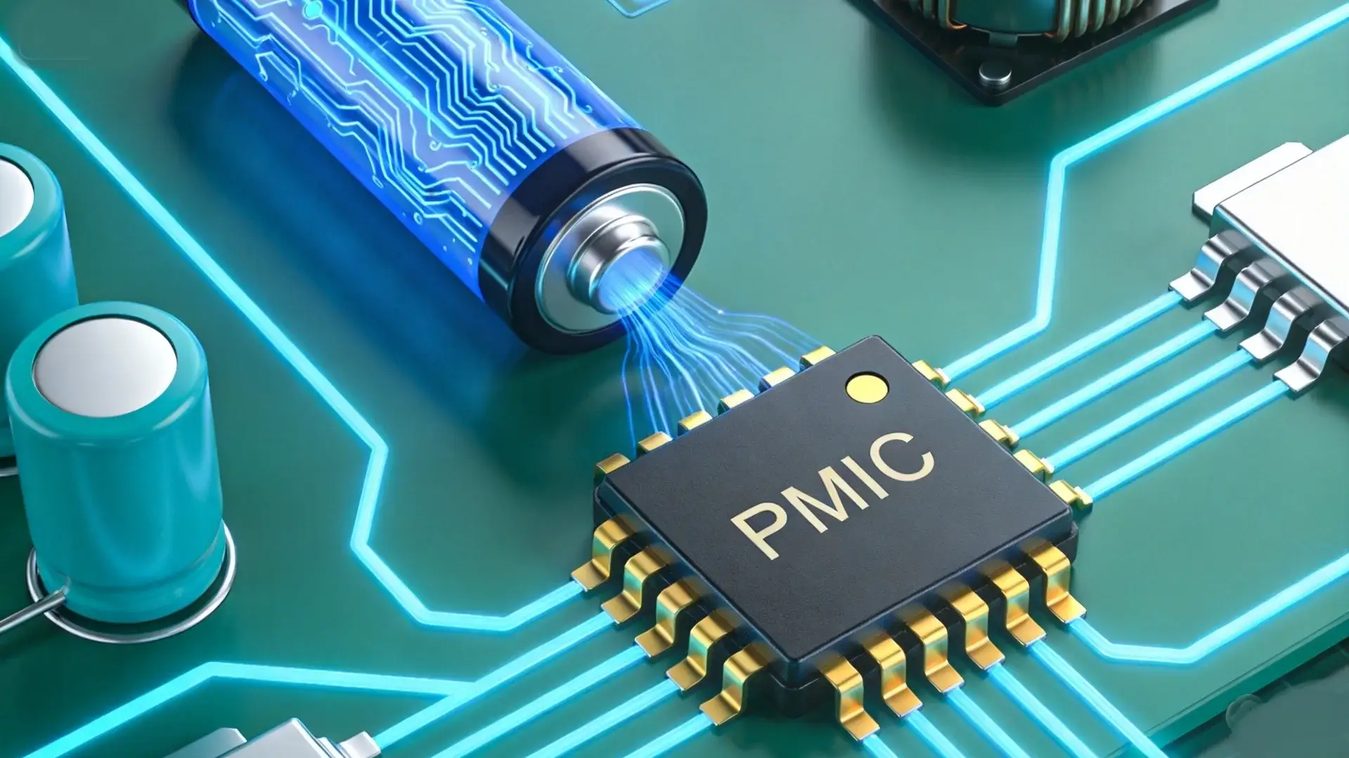
Notably, wearable manufacturing presents unique challenges beyond standard electronics assembly. Miniaturization requires specialized SMT equipment capable of placing 0201 or even 01005 components. Additionally, optical sensor calibration demands controlled lighting environments and individual unit tuning.
In fact, over 80% of global wearable production is concentrated in Shenzhen. The city’s ecosystem of sensor calibration labs, RF test houses, and component logistics creates unmatched manufacturing depth. This concentration gives founders access to rapid iteration cycles and specialized expertise that alternative locations cannot match.
When evaluating manufacturing partners, founders should verify several critical capabilities:
| Criteria | What to Check |
| Firmware ownership | OTA update access and bootloader control |
| Test transparency | Actual FCC/CE test reports, not just certificates |
| Component traceability | Batch logging for critical ICs |
| Calibration capability | Standardized light conditions for optical sensors |
| Post-launch support | Documented response SLA for bug fixes |
Cost structures also differ from standard electronics. Base wearable modules including SoC, RAM, flash, and BLE cost 15 per unit. AMOLED displays add
7, while batteries and enclosures contribute another
10. Firmware and app development typically ranges from
45,000 as a one-time investment. Certification support adds
15,000.
Mold development for wearable enclosures requires extreme precision. Micro-molding techniques handle part weights under one gram with tolerances of plus or minus 0.02mm. Therefore, manufacturing support partners must demonstrate this capability before any tooling commitment.
Testing and Certification Requirements
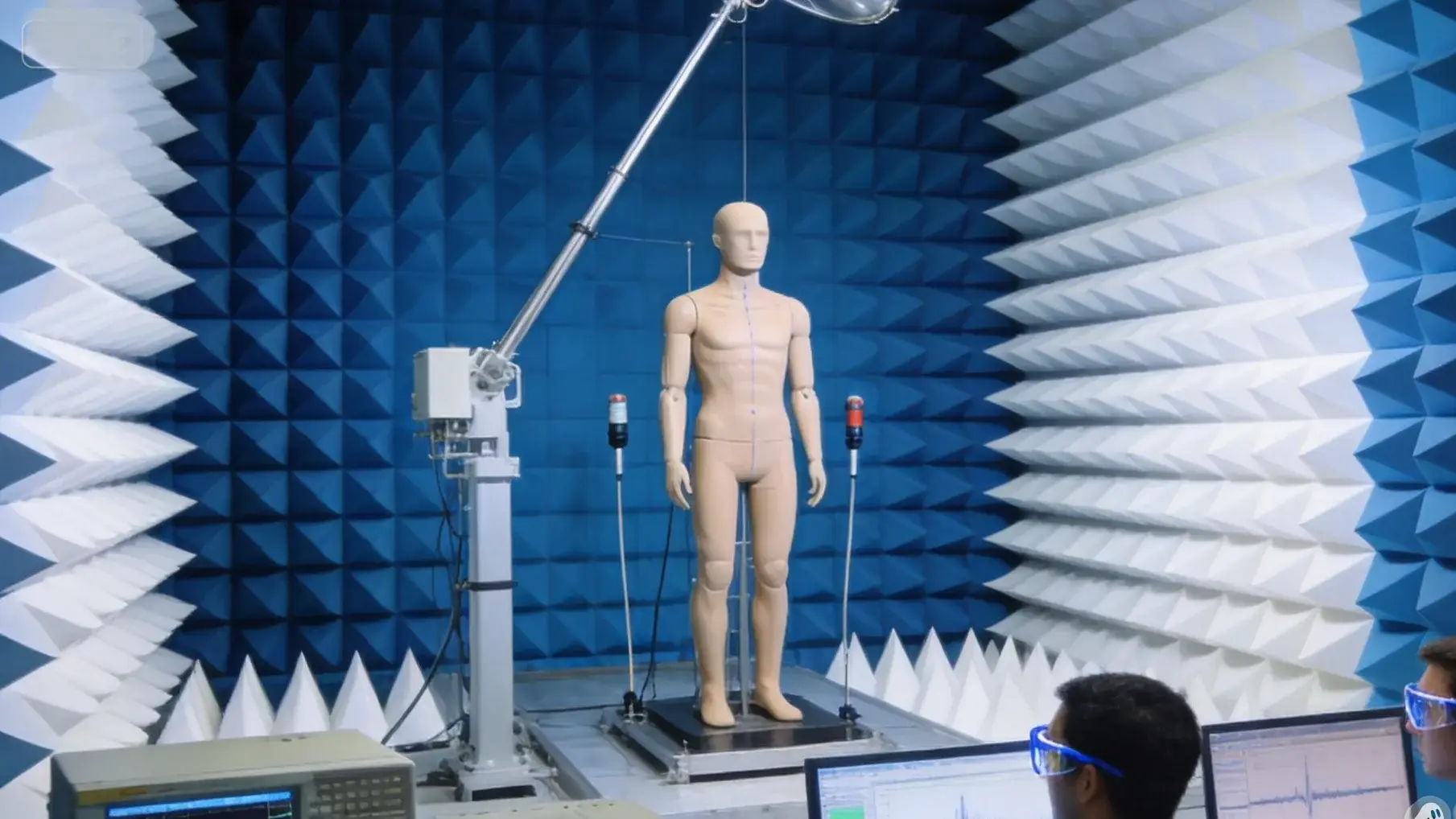
Importantly, wearable devices face a broader certification scope than most consumer electronics. Beyond standard radio compliance, wearables must meet additional safety and biocompatibility standards.
Key certifications include IEC 62368-1 for general safety and FCC Part 15B for U.S. radio compliance. The RED Directive covers European market access. Battery safety requires UN38.3 transport testing and IEC 62133-2 certification. Additionally, SAR testing is mandatory for devices worn near the body, documenting electromagnetic energy absorption limits.
Furthermore, the U.S. Cyber Trust Mark program is becoming a de facto requirement. Based on NIST IR 8425A guidelines, this program emphasizes hardware roots of trust. Major retailers like Amazon and Best Buy are moving toward stocking only certified devices. The FCC Cyber Trust Mark program requires physical secure enclaves — features that cannot be added via software patches.
Compliance certification should be planned early in the development cycle. Retrofitting security hardware into a finalized design is far more expensive than building it in from the start. Moreover, certification delays are the most common cause of missed launch dates in wearable projects. Allocating 8 to 12 weeks for lab testing and documentation prevents schedule overruns.
How OPD Design Accelerates Wearable Projects
Specifically, OPD Design brings end-to-end product development capabilities specifically suited for wearable device projects. Our integrated approach covers every stage from concept to mass production.
For wearable founders, this means working with a single team that understands the full development lifecycle. Our industrial design team optimizes for body-worn ergonomics and aesthetics. Our mechanical engineering experts handle micro-molding and precision assembly. Our hardware design specialists tackle rigid-flex PCB layout and RF optimization.
Rather than managing multiple vendors across time zones, founders work with one coordinated team. This reduces communication overhead, eliminates finger-pointing, and accelerates time to market. The result is a smoother path from first prototype to certified mass production.
FAQ
What is the typical timeline for wearable device development?
A custom wearable project takes 6 to 9 months from concept to production-ready prototype. Certification adds another 8 to 12 weeks. ODM-based projects can move faster but offer limited differentiation.
How much does wearable device development cost?
Development costs range from 250,000 depending on complexity. Key cost drivers include sensor count, firmware requirements, and certification scope. Unit costs for basic wearables start around
30 per unit.
Which connectivity protocol should my wearable use?
Most wearables use Bluetooth Low Energy for phone pairing. Add Thread or Wi-Fi based on your data bandwidth needs. For smart home integration, consider a multi-protocol SoC that supports Matter natively.
Do wearables require medical certification?
Only devices making medical claims or diagnosing conditions require FDA classification. Fitness tracking devices generally avoid this path. However, any device measuring heart rate or blood oxygen should prepare for regulatory scrutiny.
Can I manufacture wearables outside of China?
Vietnam and India are developing wearable manufacturing capacity. However, Shenzhen remains the center of gravity. The depth of sensor calibration labs and component logistics there is unmatched globally.
Start Your Wearable Project Today
Indeed, building a wearable device requires more than a great idea. It demands expertise in miniaturized hardware, biocompatible materials, power-optimized firmware, and precision manufacturing. The difference between a successful launch and a costly failure often comes down to having the right development partner.
OPD Design has guided hardware founders through every stage of wearable device development. From first concept sketch to certified mass production, our team helps you navigate the challenges. Whether you are building a fitness tracker, a medical-grade monitor, or a next-generation smart ring, we can help.
Contact us to schedule a project consultation. Take the first step toward bringing your wearable product to market.