
TL;DR — What You Need to Know in 30 Seconds
PCB design is not just about connecting components. Rather, it is the discipline that determines whether your hardware works reliably, passes certification, and can be manufactured at scale. For hardware founders, understanding the PCB design process from day one prevents costly respins. Moreover, it reduces certification delays and compresses your time to market. This guide walks through every phase: schematic capture, component selection, stackup planning, layout, DFM review, and manufacturing file preparation. By the end, you will know what to expect and what to avoid. Furthermore, you will know when to bring in an experienced hardware design partner.
| Key Takeaway | Detail |
| Design priority | Reliability and manufacturability must guide every decision |
| Most expensive mistake | Locking stackup and impedance targets after layout begins |
| Typical PCB layers | 4-layer for consumer IoT, 6-8 layers for high-speed designs |
| Test point rule | Plan test points before layout — retrofitting is painful |
| Design partner value | Reduces respins and compresses EVT timeline significantly |
Introduction: Why PCB Design Knowledge Matters for Every Hardware Founder
You do not need to be an electrical engineer to build a hardware product. However, you do need to understand how a printed circuit board works. Why? Because the decisions made during PCB design directly affect your product’s reliability, EMC performance, thermal behavior, and manufacturing cost. Indeed, a board that fails in the field destroys customer trust. Similarly, a board that cannot be manufactured reliably halts your production ramp.
The stakes are concrete. Industry data shows that PCB-related issues account for up to 40% of hardware design respins. Specifically, these include signal integrity failures, thermal overruns, and DFM violations. Each respin adds 4–8 weeks and 50,000 in costs, depending on board complexity. For a hardware startup operating on a tight 18-month runway, that is not a minor inconvenience. Rather, it is a potential business-ender.
Therefore, treating PCB design as a black box handed off to an engineer is a mistake most first-time founders make. You do not need to route traces yourself. Instead, you need to understand the process well enough to ask the right questions and catch obvious errors. In addition, you must make informed trade-offs between cost, performance, and schedule.
Ultimately, this guide gives you that foundation.
Understanding the PCB Design Workflow
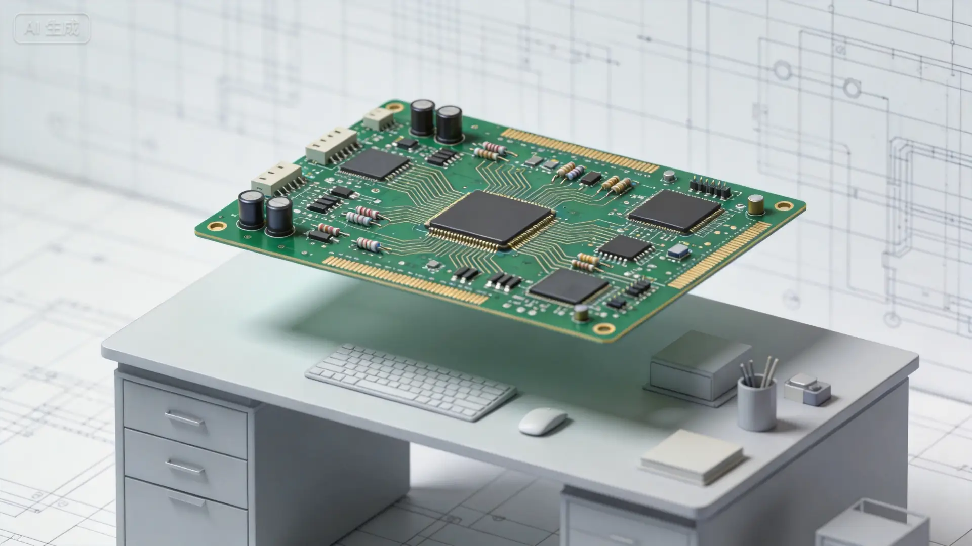
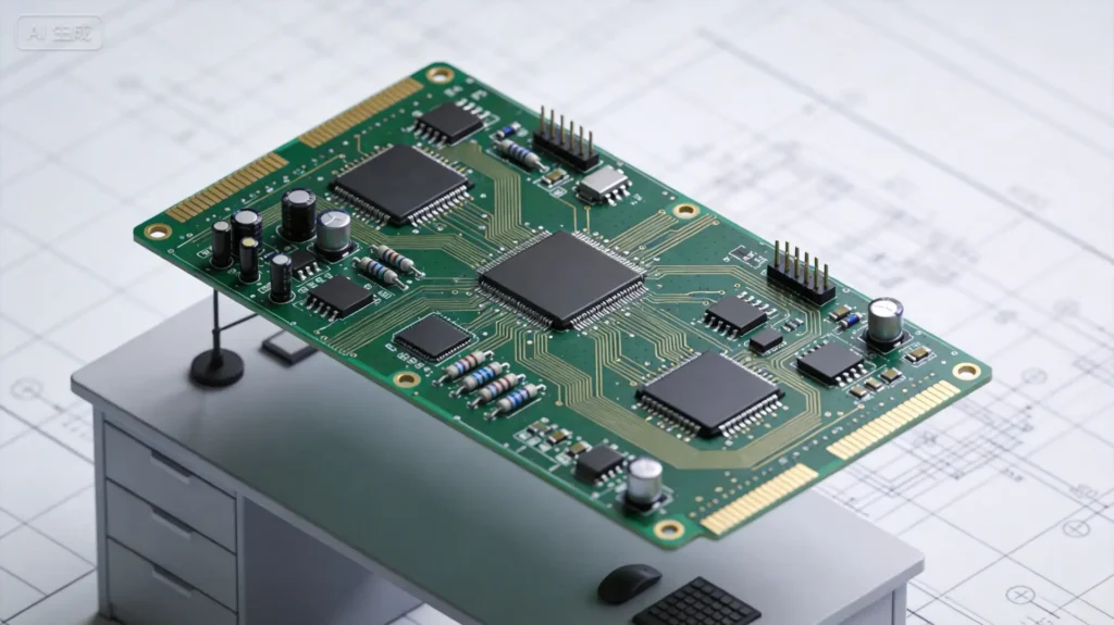
The PCB design process moves through six interconnected phases. Skipping or compressing any phase creates problems that surface later. Consequently, later always costs more.
| Phase | Duration (typical) | Key Output |
| Schematic capture | 1–3 weeks | Netlist, BOM |
| Component selection | 1–2 weeks | Approved vendor list, sourcing status |
| Stackup planning | 3–7 days | Layer stack specification |
| PCB layout | 2–6 weeks | Complete Gerber package |
| DFM review | 3–7 days | Fabrication and assembly drawings |
| Manufacturing files | 2–5 days | Gerbers, drill files, pick-and-place |
The critical insight is that schematic errors are cheap to fix. In contrast, layout errors discovered after fabrication are expensive. This is why each phase has a gate review before the next one begins.
Phase 1: Schematic Capture — Define What You Are Building
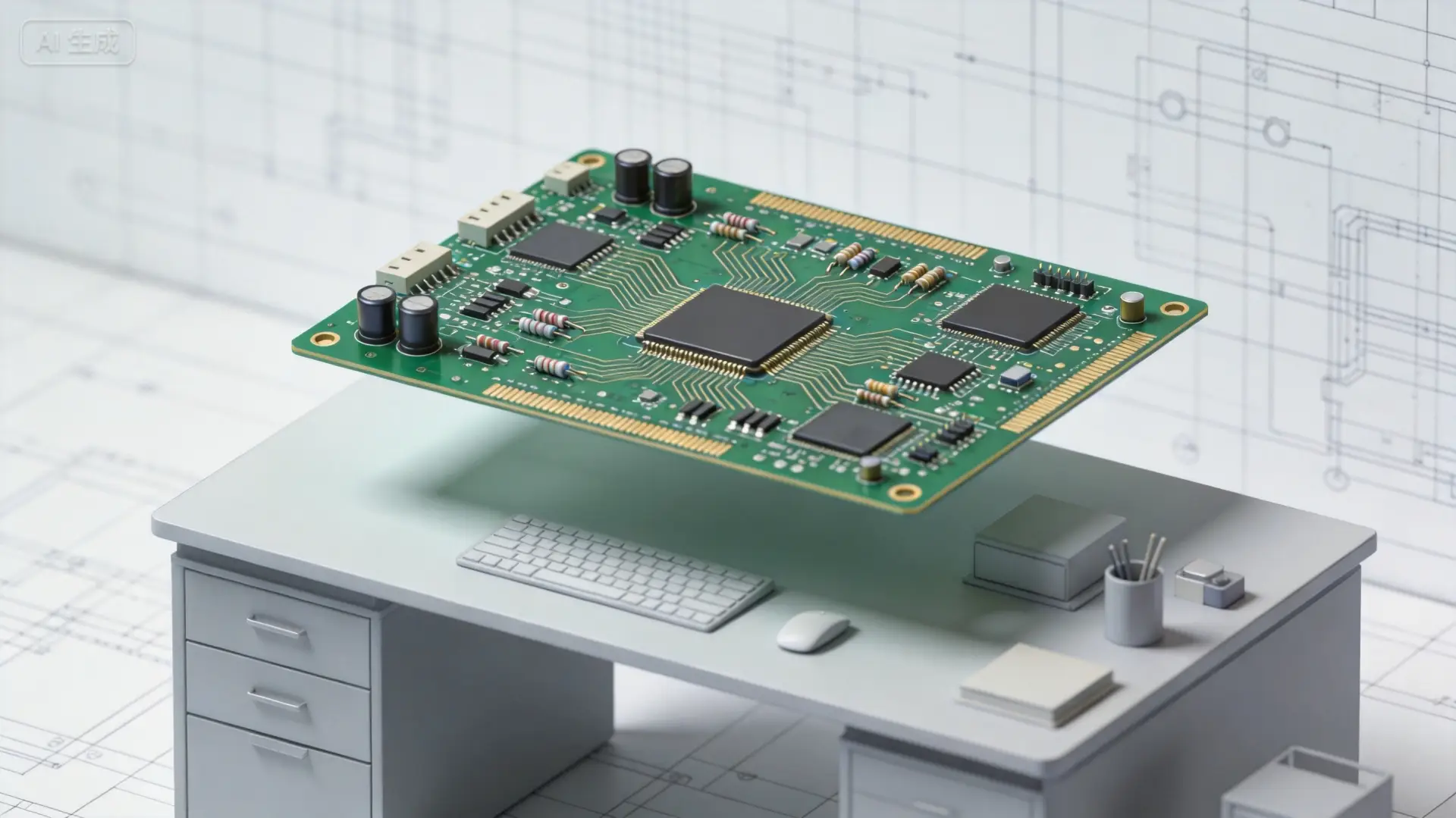
Schematic capture is the process of drawing the circuit. Specifically, it involves specifying every component, every connection, and every electrical constraint. First, this is where the circuit architecture is defined. Therefore, this phase sets the direction for everything that follows.
During schematic capture, the design team defines:
• Power distribution architecture (voltage rails, current requirements)
• Signal interfaces (USB, UART, I2C, SPI, wireless modules)
• Protection circuits (TVS diodes, fuses, reverse-polarity protection)
• Clock and oscillator placement
• Analog signal conditioning requirements
Additionally, the schematic also generates the bill of materials (BOM), which is critical for supply chain planning. Component selection at this stage must account for lead times, pricing at volume, and long-term availability. Indeed, electrical specifications alone are not sufficient. This is why BOM creation should involve your procurement or manufacturing team from day one, not after design lock.
A common founder mistake is using a component that is perfect electrically. However, it may be impossible to source at volume within your product launch window. Always validate component availability against distributor stock and manufacturer lead times before finalizing the BOM. Additionally, for complex assemblies, involving your mechanical design team early ensures the PCB fits the product enclosure without clearance conflicts.
Phase 2: Component Selection — Beyond Electrical Specifications
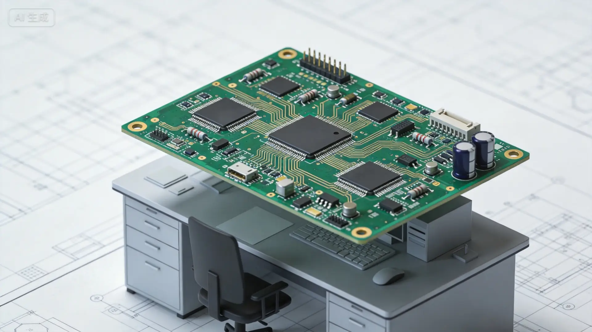
Component selection is where electrical performance, supply chain reality, and manufacturing feasibility intersect. For hardware founders, the key decision points are as follows:
Package Type
Surface-mount (SMD/SMT) components dominate modern PCB designs. Notably, they offer better automated assembly yields, smaller footprints, and lower parasitic inductance compared to through-hole parts. However, smaller packages (0201, 01005, BGA) require tighter manufacturing tolerances and increase the risk of assembly defects. Working with an industrial design partner from concept helps ensure the product form factor accommodates the PCB size. Additionally, it addresses thermal requirements from the start.
Lead-Free vs. Standard Solder
If your product will ship to Europe or require CE marking, you need lead-free assembly (RoHS compliance). Specifically, lead-free solder has a higher melting point and creates more mechanical stress on joints during thermal cycling. This matters for products that will experience wide temperature ranges or high vibration.
Component Lifecycle
Some components go obsolete quickly. In particular, this is common in the consumer IoT space where chipmakers refresh reference designs annually. Choose components with long-term availability (10+ year lifecycle). Thus, you avoid forced redesigns mid-production.
Working with an experienced hardware design company at this stage helps you balance technical requirements against supply chain realities. In fact, we maintain relationships with authorized distributors and can advise on component substitutions before they become problems.
Phase 3: Stackup Planning — The Foundation of Everything

The PCB stackup is the layered structure of copper and insulating substrate. Specifically, it is the foundation of your board’s electrical and thermal performance. It must be planned before layout begins. In other words, not after.
Layer Count Decisions
| Application | Typical Layer Count | Rationale |
| Simple microcontroller boards | 2 layers | Low cost, suitable for through-hole friendly designs |
| Consumer IoT devices | 4 layers | Dedicated power and ground planes improve EMC |
| High-speed digital (DDR, USB3) | 6–8 layers | Signal integrity requires controlled impedance |
| RF and mixed-signal | 6–10 layers | Analog shielding and isolation requirements |
Every additional layer adds cost (typically 15–25% per layer) and fabrication lead time. Therefore, your stackup should be the minimum complexity required to meet electrical and EMC requirements. In other words, avoid a safety margin that inflates cost.
Material Selection
FR-4 is the standard substrate for most boards. Notably, it offers good mechanical properties, excellent solderability, and low cost. However, for boards with high thermal demands or high-frequency signals, alternative materials become necessary.
| Material | Tg (Glass Transition) | Typical Use |
| Standard FR-4 | 130–140°C | Consumer electronics, IoT |
| High-Tg FR-4 | 150–170°C | Automotive, industrial |
| Polyimide (PI) | 240–260°C | Aerospace, high-reliability |
| Rogers RO4003C | 280°C+ | RF and microwave applications |
The choice of dielectric constant (Dk) and dissipation factor (Df) affects impedance control for high-speed signals. Accordingly, for designs targeting USB 3.0, HDMI, or DDR memory interfaces, stackup must be validated against impedance targets. This must be done before layout begins.
Phase 4: PCB Layout — Where Design Meets Physics


PCB layout translates the schematic into physical geometry. This is where electrical performance meets manufacturing reality. Importantly, it is the phase most prone to costly errors.
Component Placement Principles
Effective placement reduces routing complexity, improves signal integrity, and simplifies thermal management. The key rules are as follows:
1. Place high-power components near board edges — where external airflow is best — to maximize heat dissipation
2. Separate analog and digital circuits spatially — digital switching noise couples into analog traces if they share proximity
3. Place oscillators and clock sources near their loads — every millimeter of extra trace adds inductance and jitter
4. Leave clearance for automated assembly — typically 0.5–1 mm between adjacent components. For firmware-heavy products, coordinate placement with your software design team. Specifically, ensure debug headers, programming connectors, and JTAG interfaces are accessible after enclosure assembly.
Routing Fundamentals
• Trace width for current: Use IPC-2221 standards to calculate minimum trace width based on current and acceptable temperature rise. For example, a 5-amp power trace on 1 oz copper needs roughly 25 mils width.
• High-speed signals require impedance control: USB (90Ω differential), HDMI (100Ω differential), DDR (specific values per generation). These must be routed on designated layers with controlled dielectric thickness.
• Avoid 90-degree corners: Alternatively, use 45-degree or arc routing to reduce reflected signal at corners.
• Differential pair length matching: For USB, PCIe, and DDR interfaces, keep the positive and negative traces matched within the tolerance specified by the standard. For example, ±5 mils for USB and ±25 mils for DDR.
Thermal Management in Layout
Heat is the enemy of reliability. Consequently, components running above rated temperature fail exponentially faster. During layout, thermal vias should be placed under all power devices. This connects the top copper to internal ground and power planes. Subsequently, for high-power components, thermal pads should use arrayed via patterns (6–12 vias, 0.3 mm diameter). As a result, heat transfer to the board’s internal copper layers is maximized.
Pro Tip: Calculate junction temperatures for all power components before releasing the layout. If any component’s thermal margin is below 20°C, redesign the placement or add heatsinking before the board goes to fabrication. Retrofitting thermal solutions after prototype testing is expensive and time-consuming.
Phase 5: Design for Manufacturing — Preventing Production Failures

Design for manufacturing (DFM) is where you validate that your board can actually be built at scale. In fact, many technically elegant designs fail in production because they violate fabrication or assembly tolerances.
Critical DFM Rules
• Via size and spacing: Use standard via diameters (0.3–0.4 mm) unless the design demands micro-vias. Furthermore, non-standard via configurations increase cost by 30–50% and extend lead times by 2–4 weeks.
• Annular ring width: Every via needs a minimum annular ring of 2.5–3 mils. Notably, smaller rings risk drill breakout — where the drill bit passes through the pad — leaving an open connection.
• Trace width and spacing for copper weight: Minimum spacing rules change based on copper weight. For instance, 1 oz copper requires 5–6 mils spacing, while 2 oz copper requires 8 mils. The IPC-A-610 standard for electronics assembly defines the acceptability criteria for all solder joint conditions.
• Test point accessibility: Plan at least 0.100-inch spacing between test points. Importantly, test points must be accessible on one side of the board for in-circuit testing (ICT).
DFM Verification Steps
Before submitting files to your manufacturer:
1. Run your Gerber files through the manufacturer’s free online DFM tool
2. Verify all traces meet minimum width and spacing for the specified copper weight
3. Confirm all vias have adequate annular rings
4. Validate that the design fits standard panel dimensions (typically 18×24 inches)
5. Check layer stackup against one of the manufacturer’s standard offerings
These five steps take about 30 minutes and eliminate the majority of manufacturing surprises. Moreover, most PCB manufacturers offer automated DFM reports that flag potential issues before fabrication begins.
Phase 6: Manufacturing Files and Production Handoff

The manufacturing file package is not just Gerbers. Rather, it is a complete set of documentation that your manufacturer and assembly partner need to build your board correctly.
Required Manufacturing Files
| File | Content | Format |
| Gerber files | Copper layers, solder mask, silkscreen | RS-274X (extended Gerber) |
| Drill files | NC drill coordinates and tool sizes | Excellon |
| Bill of Materials (BOM) | All components, quantities, references | CSV or XLSX |
| Pick-and-place file | Component coordinates for assembly | CSV |
| Assembly drawing | Reference designators, orientation markers | |
| Stackup specification | Layer count, materials, thicknesses | PDF or CAD export |
The Hidden Cost of Incomplete Documentation
Boards sent to fabrication without complete documentation are routed through the manufacturer’s engineering review queue. Consequently, this adds 3–5 business days to lead time. Furthermore, a complete package eliminates this delay and reduces the risk of misinterpretation.
Our product prototyping team prepares complete manufacturing packages for every design. In particular, we include engineering reviews that catch documentation gaps before they become production delays.
Common PCB Design Mistakes Hardware Founders Should Avoid
From our experience supporting hardware startups through dozens of NPI cycles, these mistakes appear most frequently:
Mistake 1: Decoupling Capacitor Placement
Placing decoupling capacitors more than 3 mm from the power pin defeats their purpose. Specifically, the parasitic inductance of the trace becomes too large to suppress high-frequency switching noise. Therefore, always place decoupling caps as close to the IC pins as the routing allows.
Mistake 2: Ignoring Impedance Matching for High-Speed Signals
USB, HDMI, PCIe, and DDR interfaces have strict impedance tolerances. Designing these traces without specifying impedance requirements in the stackup leads to signal reflections and eye diagram failures. Furthermore, it creates EMC problems that cannot be fixed in firmware.
Mistake 3: Single-Point Ground for Mixed-Signal Designs
Analog and digital grounds must be tied at a single point — typically near the power entry. Otherwise, tying them at multiple points creates ground loops that inject digital switching noise into analog measurement circuits.
Mistake 4: Insufficient Power Plane Current Capacity
Power planes must be sized for the total current they carry. Undersized power planes cause voltage droop under load transients, leading to processor resets and erratic sensor readings. Therefore, use copper weight calculators (IPC-2221 or IPC-2152) to verify plane current capacity.
Mistake 5: Not Planning for Panelization
Boards designed without considering panelization (how multiple boards are arranged on a fabrication panel) waste material and increase per-unit cost. Standard panel dimensions are 18×24 inches or 24×30 inches. Consequently, boards with non-standard aspect ratios or oversized dimensions cannot be efficiently panelized.
When to Engage a Hardware Design Partner
PCB design requires deep expertise in circuit theory, electromagnetic compatibility, thermal engineering, and manufacturing processes. Most hardware startups do not have this expertise in-house. Indeed, building it takes years.
Indeed, engaging an experienced hardware design partner offers concrete benefits:
• Reduced respin cycles: Expert layout engineers know DFM rules and EMC principles from experience, not just from documentation. As a result, this eliminates the trial-and-error that inflates timelines for first-time hardware teams.
• Accelerated EVT timeline: Getting to first functional prototype faster compresses the entire NPI process. Subsequently, you gain more time for user testing and iteration.
• Certification readiness: Good PCB design is a prerequisite for CE, FCC, and UL compliance. Conversely, boards designed without EMC principles in mind require expensive shielding and filtering fixes after certification testing.
• Supply chain integration: Experienced partners maintain relationships with component distributors. Consequently, they can source alternatives quickly when primary components go obsolete.
OPD Design provides end-to-end hardware design services. Specifically, we cover schematic review, component selection, layout, DFM, and manufacturing file preparation. We work alongside your team through every phase. As a result, your board is designed for production from the first prototype onward.
Ready to build your next hardware product with a partner who understands PCB design from schematic to scale? Contact OPD Design to discuss your project requirements. We offer free initial consultations for hardware startups building in consumer electronics, IoT, medical devices, and industrial equipment.
Frequently Asked Questions
What is the typical cost of PCB design for a consumer IoT product?
PCB design costs vary widely based on complexity and layer count. Additionally, the cost depends on whether you hire a freelancer, an agency, or an integrated design partner. A 4-layer consumer IoT board typically costs 15,000 for design and layout. High-speed or RF designs with 6–8 layers range from
40,000. Notably, these figures cover schematic, layout, and DFM review — not prototyping or certification testing.
How long does it take to design and manufacture a PCB?
A simple 2–4 layer board can go from schematic to assembled prototype in 4–8 weeks with an experienced team. In contrast, a complex 6–8 layer board with high-speed interfaces typically requires 8–16 weeks. Furthermore, the manufacturing phase (fabrication + assembly) adds 2–4 weeks on top of design time.
What is the difference between a prototype PCB and a production PCB?
Prototype PCBs are typically manufactured with standard tolerances, often as single units or small panels. Moreover, they use the fastest available fabrication options. Production PCBs are optimized for panel efficiency, solder paste compatibility, testability, and long-term reliability. In contrast, prototype boards sometimes mask manufacturing issues that surface only at volume production scale.
Can I use open-source hardware designs as a starting point?
Yes, many founders use reference designs from chip vendors (TI, STMicroelectronics, NXP, Espressif) as starting points for their schematics. However, reference designs are not production-ready. Instead, they must be adapted for your specific form factor, thermal environment, regulatory requirements, and supply chain constraints. Ultimately, treat them as a learning foundation, not a finished product.
What certifications require PCB-level compliance testing?
Most electromagnetic compliance certifications (CE/FCC Part 15, for example) require pre-compliance testing at the PCB level. Specifically, this must be done before submitting for formal certification. Boards with poor EMC design often fail certification testing and require expensive retrofits. For example, shielding cans, ferrite beads, and filter components add cost and weight. Ultimately, designing for EMC from the start is far cheaper than fixing it after certification failure.